PCB prototyping machine and engraver: start etching your own PCBs
PCB DIY: make your own PCBs. Save money. Be fast.
Laser engraving with PCBs
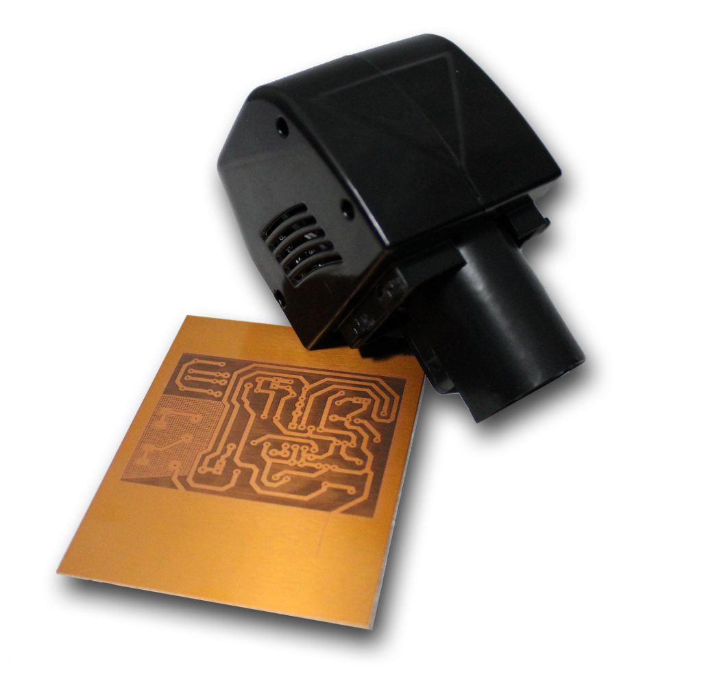
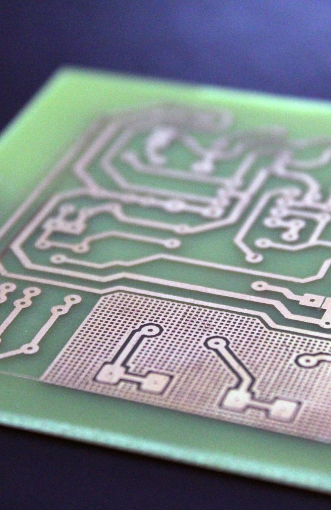
PCB laser engraving is the process of removing a fine layer off a photosensitive board with a laser beam to expose the copper beneath.
The copper is subsequentially corroded by means of an acid bath.
With this method a fully-fledged PCB can be ready for SMT soldering in very little time, saving in development time.
This method is the one shown in the samples, which are made with a negative photosensitive board.
Differently, the laser beam hitting a positive photosensitive PCB will polimerize a fine layer that will not be eroded by the acid bath.
The two alternatives make possible to work on different PCBs with same precise results.
Both are widely available and extremely cheap.
Precision for SMT components
Surface Mount Technology (SMT) is obiquitus nowadays.
PCB prototyping with the FABtotum Laser Head is capabale of reaching the precision and tolerance required for this technology.
Creating a prototype with SMT technology means getting to pre-production without the need of developing a separate “proof of concept” board for internal use or to wait weeks to validate a design.
The Laser Head is used internally by our R&D team to assess and validate new electronic applications and HW designs on a daily basis.
With the Laser Head a significant part of the prototyping stage is skipped alltogether.
You are welcome to try that out!
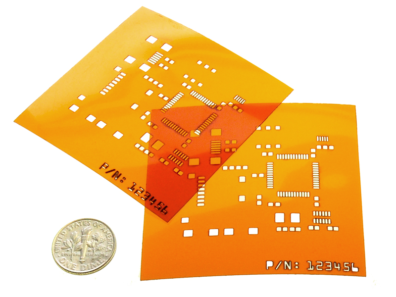
Making Solder Paste Stencils for reflowing.
As said, surface Mount Technology (SMT) is obiquitus nowadays.
Every PCB manufactured with this tecnique also require a precise control on where the solder paste is deposited.
This is where solder paste masks came handy: they provide a way to effectively and easily prepare the PCB for solder SMT components with the reflow technique.
Contrary to manual soldering, with this tecnique an entire board and most of its SMT components on the same side are soldered at once.
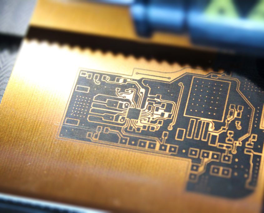
With the laser head you can effectively laser-cut stencils starting from the PCB design program you normally use and by exporting the outlines in a vector format.
Just postprocess it with our software, then start cutting the mask on your FABtotum Personal Fabricator equipped with the Laser Head.
Preparing a solder mask can take a few minutes but it greatly reduces the soldering time and effort required to manually solder each and every component to the board and, best of all, it does not require expensive materials or extra equipment.
Cost Savings, solutions compared
Say goodbye to pesky setup costs and time delays when producing samples with PCB manufacturers.
With the Laser Head it’s possibile to cut costs and time to a fraction.
Up to 2 layers the advantages are groundbreaking.
A unified prototyping platform
With the FABtotum Personal fabricator and the Laser Head you can support your prototyping and small production needs.
A few examples:
- With the Laser Head you can cut a solder mask and use it to distribute solder paste on your PCB
- With a FABtotum 3D Printing Head you can design, print and test an enclosure for your PCB in a matter of few hours.
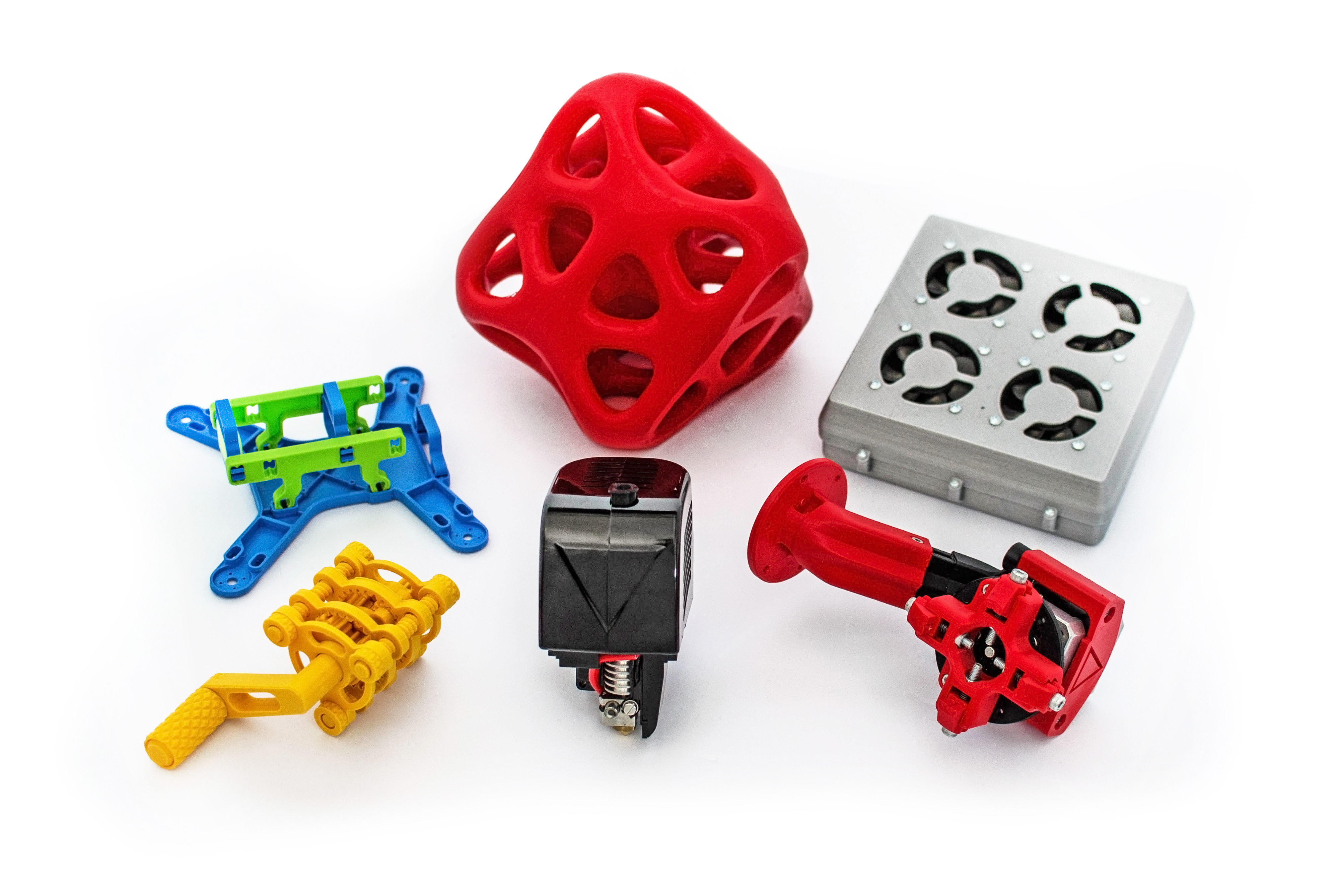
- You can create mechanical parts and components for your application.
- By indexing the origin point it’s possible to create two-sided PCBs as well
- Using the Laser Head in conjunction with the Milling Head it is possible to drill PCBs or to cut the profile and separate the PCB from the rest of the copper board before or after treatment.
