PCBs making with FABtotum
How To: Single sided PCB laser etching with FABtotum Core and its Laser Head.
To create a PCB, using photosensitive boards and a FABtotum Core, you need tools and devices as follows:
• FABtotum Core (or previous version)
• Laser Head
• Photosensitive Copper Board
• Sodium hydroxide (NaOH)
• Ferric acid (FeCl3)
• Latex gloves
• Trays and pliers of non-metallic material
You should always operate in a well-ventilated area and wear a workwear and latex gloves. The process involves the following steps:
1. Extraction of MASTER ARTWORK from electronic CAD software;
2. Convert MASTER ARTWORK to a compatible format for the FABtotum application for PCBs;
3. Upload the MASTER ARTWORK on the FABtotum’s online application for PCBs;
4. Etching of the PCB with FABtotum and LASER head;
5. Board envelope;
6. Drilling, cutting and assembling components.
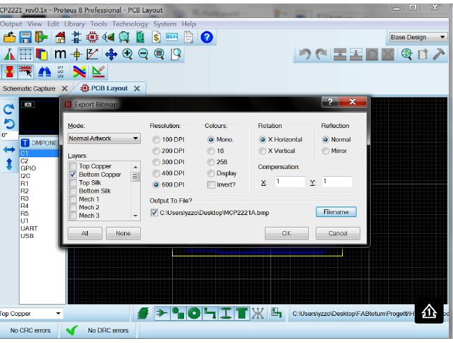
The extraction of the MASTER ARTWORK for convenience is made in image format, this option is available on most electronic CADs. In the used software, for example, the export of MASTER ARTWORK is in .bmp format:
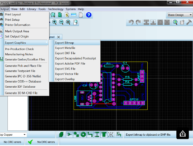
Choose the highest resolution, which should be 600 DPI and select only the layers you need for the engraving: “bottom copper” and “board edge”:
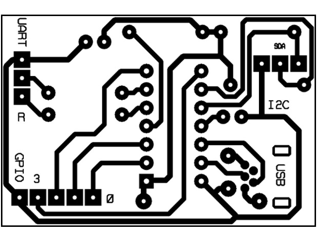
Make sure to know the width of the PCB; the image should look like the one here below:
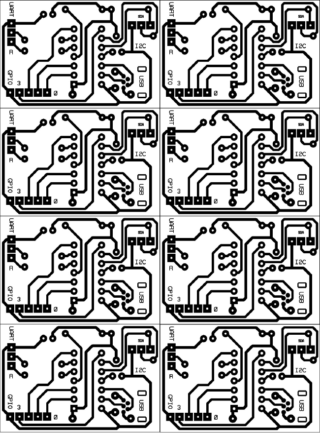
In case of a multi PCB board, with a simple photoeditor (Paint works fine as well) it is easy to make a small panelizing as the one you can see below. Make sure to calculate the right width again:
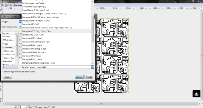
Next step is to convert the image into a file that FABtotum app can correctly postprocess. The chosen extension is .jpeg. You will need a again a photo editor: a free and open source example is GIMP.
The image below shows how to export the file to jpeg.
You then need to load the .jpeg file on FABtotum’s online app in order to correctly generate the GCODE for laser engraving:
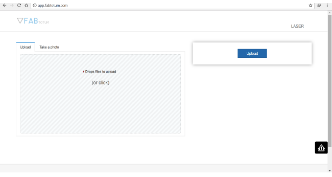
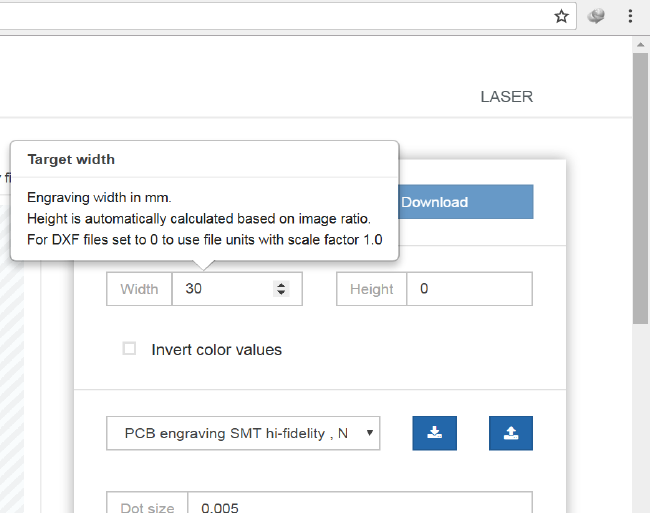
Upload the image and make sure to write the final width of the PCB in the shown box:
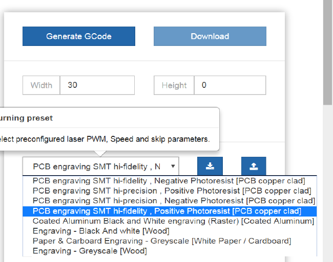
Choose the right profile, this time you’ll pick “PCB engraving SMT hi-fidelity, Positive Photoresist [PCB copper ciad]”, then generate the g-code:
Once you have the gcode and you have it saved on your pc, upload it on the FABtotum. Place the photosensitive board on the Hybrid Bed and the tip of the Laser Head 2mm far from the board. The task will (always) start from front-left corner. The entire etching process should be run with low or no lights to gain precision and increase final quality.
Once the engraving is completed, dip the board in a solution of water and Sodium hydroxide in a percentage between 5 and 10%.
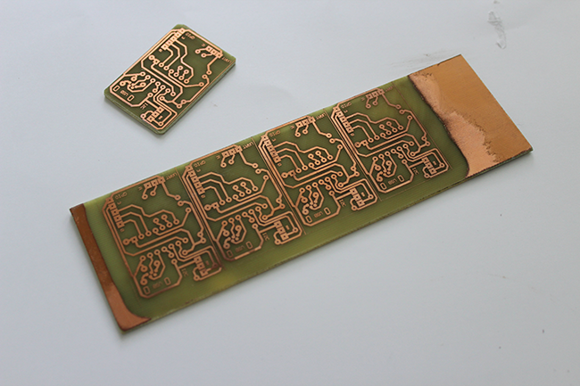
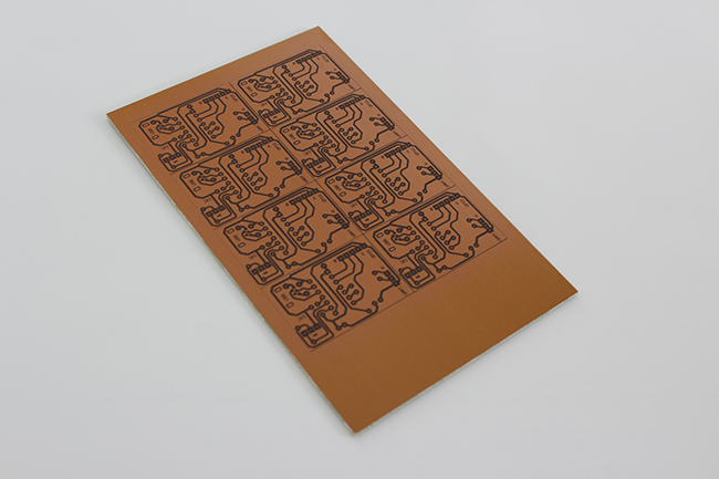
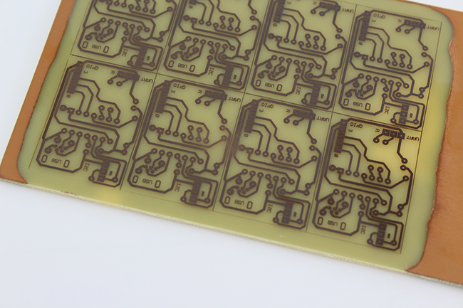
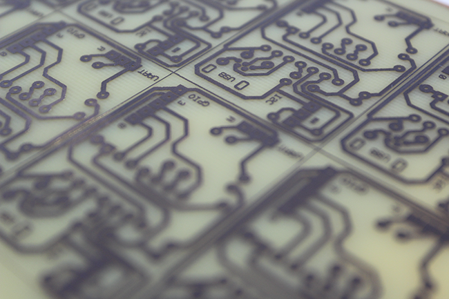
The process will take less than a minute: hydroxide will remove the unnecessary photoresistant material (the one that has not been lasered), leaving the PCB MASTER clearly visible:
Rinse the board with water, dry it.
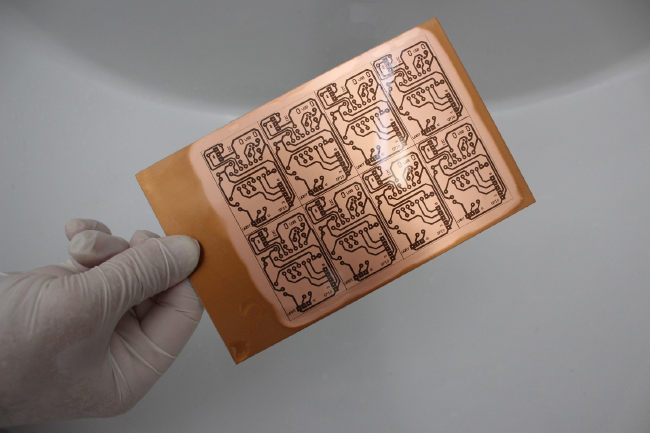
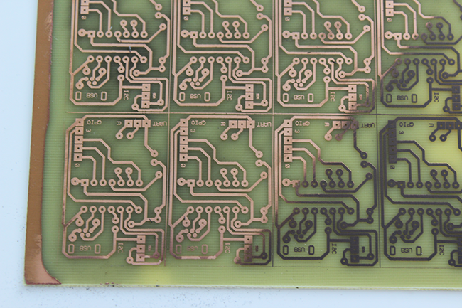
You will then need to proceed with dipping the board into ferric acid: this will remove the copper layer that has not been lasered and is not a part of the “MASTER ARTWORK”. After this step the pattern will be even clearer.
The ferric acid must be enough to cover the whole board (but avoid adding too much in order to preserve quality of the final work). The copper erosion process depends on the dimension of the board; it takes more than 10 minutes:
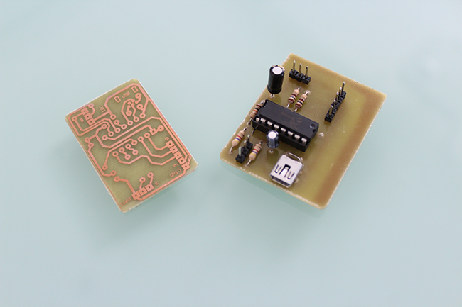
Rinse and dry the board again, then clean it with acetone:
Next steps are cutting, drilling and soldering components: to drill the vias you can use the Milling Head, but that’s another story!